What happened
- A team from Huazhong University of Science and Technology and the Optics Valley Laboratory, in Wuhan, China, published in Nature on October 28, 2026 a method for growing lead sulfide infrared detectors directly on the integrated circuit that reads their signals.
- The process takes place in water at room temperature and is inspired by biomineralization, the way living things form minerals such as shells and bones.
- With antimony doping, the photodiodes reached a specific detectivity of 4.4 × 10¹¹ Jones at 2.5 micrometers, above that of commercial indium gallium arsenide detectors, according to the paper.
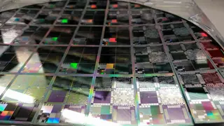
- The team built a 640 by 512 pixel array that captures clear infrared images and integrated devices onto flexible readout circuits.
Why it matters
- Infrared cameras are built today by bonding a detector array to a readout circuit, a step that adds complexity and cost. Growing the detector on the circuit removes it.
- Until now, depositing the material from a solution failed to produce electronic-grade films without damaging the circuit. The authors managed it by regulating how lead binds to hydroxyl groups in water and by shielding the process from environmental disturbances.
- The result is quasi-single-crystal films, uniform at wafer and pixel scale, with a carrier density of about 2 × 10¹⁵ per cubic centimeter and a mobility of 124 cm²/V·s.
- The 2.5 micrometer range corresponds to short-wave infrared, used in night vision, industrial inspection, agriculture and vehicle sensors.
The number
640 × 512 pixels. That is the resolution of the focal-plane array the team built with the new process.
Context
Lead sulfide is a well-known infrared detection material and occurs in nature as galena. Its appeal is cost: indium gallium arsenide, standard in this band, requires expensive growth processes and does not integrate easily on silicon.
The authors frame their work within demand for image sensors for AI systems, which need to see in conditions where visible light falls short. They call the method monolithic in situ integration, because the detector is born on the circuit rather than attached afterward.
Integration on flexible circuits opens another line, curved or conformable infrared sensors, although the paper presents it as a demonstration rather than a product.
What’s next
- The long-term stability of the films and manufacturing yield at industrial scale are still unknown.
- The comparison with commercial detectors was made at one wavelength; performance across the infrared range will need more measurements.
Bottom line
Cheap infrared is a shared goal: quantum dot photodiodes matched indium gallium arsenide ones. In chipmaking, Shanghai tested a two-stage flat optic for EUV lithography, and in new devices, a sleeve with pixel fibers displays video and supertwisted WS₂ layers respond to polarized light.
Sources
- Nature — Monolithically and in situ integrated PbS infrared imagers (Li et al., October 28, 2026)
- Cover image: Ivar Leidus, CC BY-SA 4.0, via Wikimedia Commons
Edited by Rodrigo Cornejo. How we select and verify: who writes these notes.