What happened
- On October 23, 2026, Nature Communications published a method to make supertwisted multilayers of tungsten disulfide, WS₂, without the central singularity left by earlier methods.
- In these structures each atomic layer is rotated by the same angle relative to the one below, which gives them chirality, a preferred direction of twist, that interacts with light.
- Conventional growth produces spirals with a defect at the centre and in-plane strain. The team, from Peking University and Taiyuan University of Technology, used a dome-shaped WS₂ monolayer as a template.
- The crack that forms on the dome acts as a dislocation line. Its two ends work as a pair of opposite-handed screw dislocations that guide layer-by-layer growth.
Why it matters
- Without the central topological defect and with little residual strain, the multilayers are more uniform, a condition for use in devices.
- The layers showed linear circular dichroism of up to 10 millidegrees and second-harmonic circular dichroism of 0.81, at a thickness of about 6 nanometres.
- Circular dichroism measures the difference in response to left- and right-polarised light, the basis of chiral photonics.
The number
6 nanometres. Approximate thickness of the multilayers that reached a second-harmonic circular dichroism of 0.81.
Context
Van der Waals materials are sheets a few atoms thick stacked together by weak forces, which allows the angle between layers to be controlled. The authors present their technique as a direct growth route for supertwisted multilayers and a programmable platform for chiral photonics. Control of electron behaviour in solids saw another recent advance: Columbia trapped electron waves in a metal through interference.
What’s next
- The authors propose the method as a platform for nanometre-thick chiral optical devices.
- The technique still has to be tested with other layered materials and different twist angles.
Bottom line
A crack in a dome one atom thick ended up guiding the growth of a defect-free twisted crystal. Precision physics had other recent results: Northwestern trapped a single positron, a quantum speed limit for thermalisation was proved and an Oxford physicist reviewed what tests of the Born rule assume.
Sources
- Nature Communications — Singularity-free supertwisted atomic layers with giant circular dichroisms (October 23, 2026)
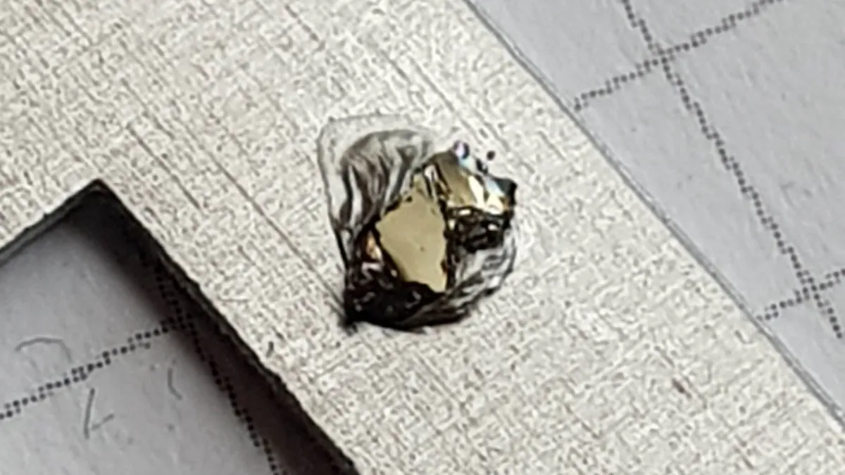
- Cover image: Fador789, CC BY-SA 4.0, via Wikimedia Commons
Edited by Rodrigo Cornejo. How we select and verify: who writes these notes.